English


The Importance of Cleanrooms in Semiconductor Manufacturing
It is a scenario that everyone is familiar with: you are using your cell phone to look up information – a street address, telephone number or very crucial TV trivia and your device freezes. Or worse, it shuts off entirely. Likely, the episode doesn’t stop there but continues to plague you until the phone is fixed or replaced. What causes this to happen?
To understand what goes wrong, one must first understand how a cell phone chip – the brain and communicator of the entire phone – is made. And to understand that, one must be familiar with semiconductors and the way they are manufactured.
Semiconductors are crystalline or glassy solids with distinct electrical characteristics. They are defined by their unique conductive behavior, somewhere between metal and insulator. Their electrical properties can be modified to allow amplification and energy conversion. Devices that use semiconductors pass currents more easily in one direction than the other with variable resistance and sensitivity to light or heat.
To manufacture electronic technology, such as a cellular phone, semiconductors for integrated circuits are produced. This process begins with one of the most common elements on earth, silicon. Silicon is found primarily in sand and from there is refined to 100% purity before it qualifies for manufacturing. Absolute clarity is necessary to produce chips that function properly. Even the slightest imperfection can radically affect the quality of the manufactured product.
To achieve this, pure silicon is heated until it reaches a molten state. Next, a perfectly structured silicon “seed” is lowered into the molten silicon. The chemical properties of the molten silicon allow a chemical bond to be formed between the seed and the chunk of solid silicon, which can slowly be pulled from the silicon as it cools, forming and solidifying around the seed. When the process is complete, the finished portion, a block, will mimic the physical characteristics of the original seed matter. The block is then carefully sawed into thin wafers.
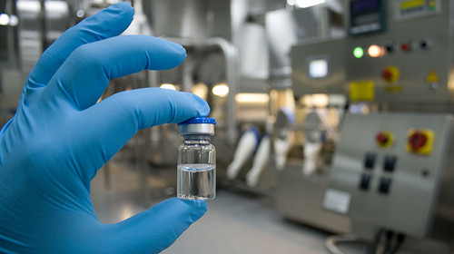
After all production steps are complete, a final protective layer is put over the entire wafer. With dimensions so minuscule, even the tiniest speck of dust can destroy the functionality of an entire chip.1 In order to accomplish this, pristine working conditions must be employed; hence, the creation of the “Cleanroom”.
A cleanroom is an environmentally controlled environment where products are manufactured. Cleanrooms are defined as specially constructed, enclosed spaces where contaminants in the air are highly controlled with respect to airborne particulates, temperature, humidity, air pressure, airflow patterns, air motion, vibration, noise, living organisms, and lighting.
The Importance of Cleanrooms in Semiconductor Manufacturing
The level to which these particles need to be removed depends upon the standards required. The most frequently used standard is the International Organization for Standardization, ISO 14644 which establishes standard classes of air cleanliness for airborne particulate levels in cleanrooms and clean zones. Strict rules and procedures are to prevent contamination of the product. 2 Without effective control, contamination can wreak havoc on products and processes.

 3rd Floor, No. 259, Juxing Road, Ximei Chenggong Development Zone, Nanan, Quanzhou, Fujian, China.
 362300
 15980759210
For inquiries about our products or pricelist, please leave to us and we will be in touch within 24 hours.


Copyright © 2024 Nanan Jiedao Electronic Material Co.,Ltd.. All Rights Reserved. Powered by

IPv6 network supported